- 您现在的位置:买卖IC网 > Sheet目录323 > EFM32G-DK3550 (Energy Micro)KIT DEVELOPMENT EFM32 GECKO
...the world's most energy friendly microcontrollers
7.3.1 User Data (UD) Page Description
This is the user data page in the information block. The page can be erased and written by software. The
page is erased by the ERASEPAGE command of the MSC_WRITECMD register. Note that the page is
not erased by a device erase operation. The device erase operation is described in Section 6.4 (p. 23) .
7.3.2 Lock Bits (LB) Page Description
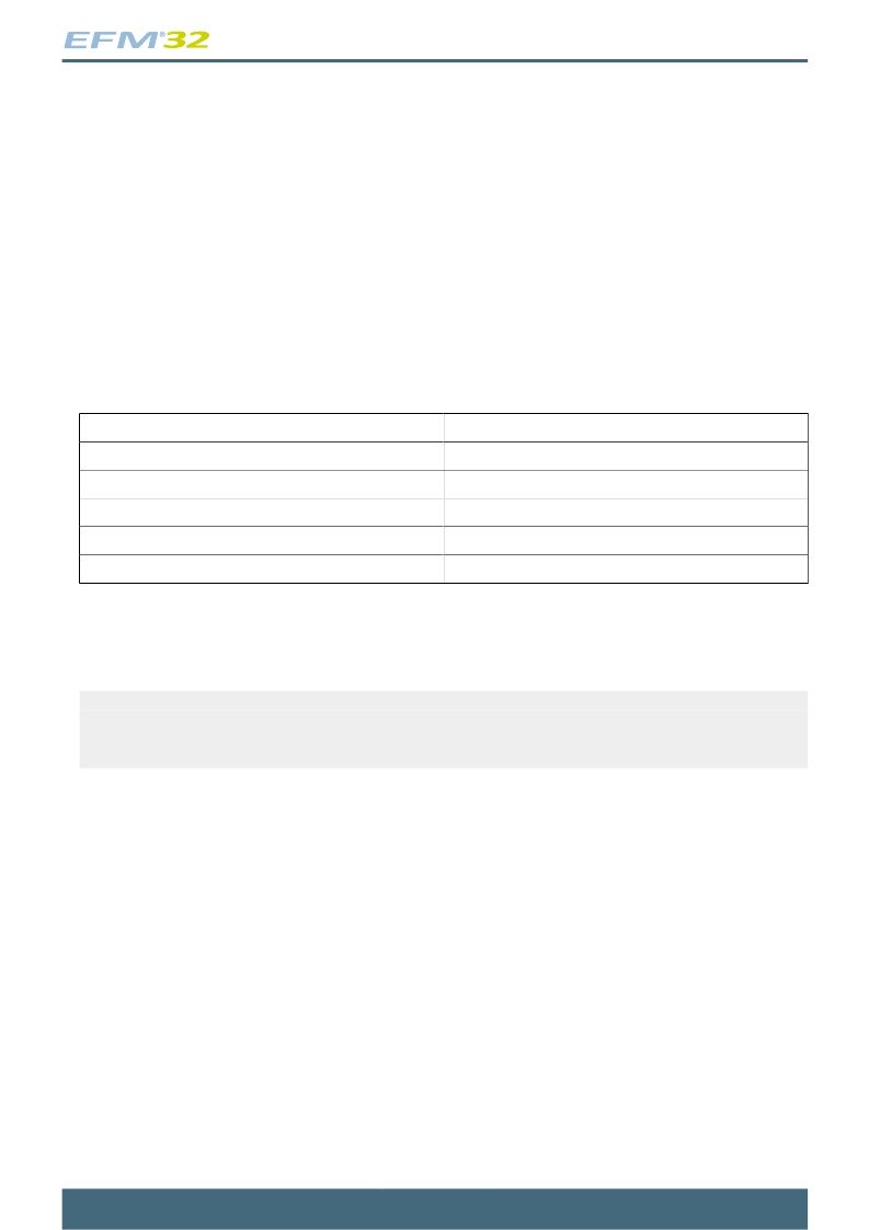
This page contains the following information:
? Main block Page Lock Words (PLWs)
? User data page Lock Word (ULWs)
? Debug Lock Word (DLW)
Table 7.2. Lock Bits Page Structure
127
126
N
…
1
0
DLW
ULW
PLW[N]
…
PLW[1]
PLW[0]
There are 32 page lock bits per page lock word (PLW). Bit 0 refers to the first page and bit 31 refers
to the last page within a PLW. Thus, PLW[0] contains lock bits for page 0-31 in the main block, PLW[1]
contains lock bits for page 32-63 etc. A page is locked when the bit is 0. A locked page cannot be erased
or written.
Note
Trying to write to a locked page before writing to a page which is not locked will write the
data that was attempted to write in the locked page. The recommended procedure if to
perform the write twice.
Word 127 is the debug lock word (DLW). Bit 0 of this word is the debug lock bit. If this bit is 1, then
debug access is enabled. Debug access to the core is disabled from power-on reset until the DLW is
evaluated immediately before the Cortex-M3 starts execution of the user application code. If the bit is
0, then debug access to the core remains blocked.
Word 126 is the user page lock word (ULW). Bit 0 of this word is the page lock bit. The lock bits can
be reset by a device erase operation initiated from the Authentication Access Port (AAP) registers. The
AAP is described in more detail in Section 6.4 (p. 23) . Note that the AAP is only accessible from the
debug interface, and cannot be accessed from the Cortex-M3 core.
7.3.3 Device Information (DI) Page
This read-only page holds oscillator, DAC and ADC calibration data from the production test as well as
7.3.4 Device Revision
The device revision number is read from the ROM Table. The Revision number is extracted from the
PID2 and PID3 registers, as illustrated in Figure 7.1 (p. 30) .The Rev[7:4] and Rev[3:0] must be
combined to form the complete revision number Revision[7:0].
2011-04-12 - d0001_Rev1.10
29
www.energymicro.com
发布紧急采购,3分钟左右您将得到回复。
相关PDF资料
EFM32GG-STK3700
KIT STARTER GIANT GECKO
EFM32LG-DK3650
KIT DEV EFM32 LEOPARD GECKO
EK-K7-KC705-CES-G-J
KINTEX-7 FPGA KC705 EVAL KIT
EK-S6-SP601-G
KIT EVAL SPARTAN 6 SP601
EK-S6-SP605-G
KIT EVAL SPARTAN 6 SP605
EK-V6-ML631-G-J
VIRTEX-6 HXT FPGA ML631 EVAL KIT
EK-V7-VC707-CES-G
VIRTEX-7 VC707 EVAL KIT
EK-Z7-ZC702-CES-G
ZYNQ-7000 EPP ZC702 EVAL KIT
相关代理商/技术参数
EFM32GG230F1024
功能描述:ARM微控制器 - MCU 1024KB FL 128KB RAM
RoHS:否 制造商:STMicroelectronics 核心:ARM Cortex M4F 处理器系列:STM32F373xx 数据总线宽度:32 bit 最大时钟频率:72 MHz 程序存储器大小:256 KB 数据 RAM 大小:32 KB 片上 ADC:Yes 工作电源电压:1.65 V to 3.6 V, 2 V to 3.6 V, 2.2 V to 3.6 V 工作温度范围:- 40 C to + 85 C 封装 / 箱体:LQFP-48 安装风格:SMD/SMT
EFM32GG230F1024G-E-QFN64R
功能描述:IC MCU 32BIT 1MB FLASH 64QFN 制造商:silicon labs 系列:Giant Gecko 包装:剪切带(CT) 零件状态:在售 核心处理器:ARM? Cortex?-M3 核心尺寸:32-位 速度:48MHz 连接性:I2C,IrDA,智能卡,SPI,UART/USART 外设:欠压检测/复位,DMA,POR,PWM,WDT I/O 数:56 程序存储容量:1MB(1M x 8) 程序存储器类型:闪存 EEPROM 容量:- RAM 容量:128K x 8 电压 - 电源(Vcc/Vdd):1.98 V ~ 3.8 V 数据转换器:A/D 8x12b,D/A 2x12b 振荡器类型:内部 工作温度:-40°C ~ 85°C(TA) 封装/外壳:64-VFQFN 裸露焊盘 供应商器件封装:64-QFN(9x9) 标准包装:1
EFM32GG230F1024-QFN64
制造商:Energy Micro AS 功能描述:GIANT GECKO MCU - Cut TR (SOS) 制造商:Energy Micro 功能描述:GIANT GECKO MCU 制造商:Energy Micro AS 功能描述:IC MCU 32BIT 1MB FLASH 64QFN
EFM32GG230F1024-QFN64T
制造商:Energy Micro AS 功能描述:GIANT GECKO MCU - Trays
EFM32GG230F1024-QFN64-T
制造商:Energy Micro AS 功能描述:IC MCU 32BIT 1MB FLASH 64QFN
EFM32-GG230F1024-SK
制造商:Energy Micro AS 功能描述:GIANT GECKO SAMPLE KIT - Bulk
EFM32GG230F1024-T
制造商:Energy Micro AS 功能描述:IC MCU 32BIT 1MB FLASH 64QFN
EFM32GG230F512
功能描述:ARM微控制器 - MCU 512KB FL 128KB RAM
RoHS:否 制造商:STMicroelectronics 核心:ARM Cortex M4F 处理器系列:STM32F373xx 数据总线宽度:32 bit 最大时钟频率:72 MHz 程序存储器大小:256 KB 数据 RAM 大小:32 KB 片上 ADC:Yes 工作电源电压:1.65 V to 3.6 V, 2 V to 3.6 V, 2.2 V to 3.6 V 工作温度范围:- 40 C to + 85 C 封装 / 箱体:LQFP-48 安装风格:SMD/SMT
